Trapping Radiation – Multiple Reflections for EMI Shielding
Innately poor film morphology during thermal evaporation can trap radiation, significantly boosting a metal’s electromagnetic interference (EMI) shielding performance. Unlike high-quality, dense metal films that primarily rely on reflection for shielding, films deposited by thermal evaporation often have a porous or nanostructured morphology. This intrinsic nanostructure enhances shielding through multiple internal reflections and absorption mechanisms, which trap and dissipate electromagnetic waves within the film itself.
Shielding mechanisms in thermal evaporation
High-quality, dense metal shields primarily block EMI through reflection due to their high electrical conductivity. However, the less-dense, intrinsically nanostructured films produced by thermal evaporation offer additional, absorption-based shielding benefits.
The “innate radiation trapping” effect is based on the following mechanisms:
- Multiple internal reflections: The porous or nanostructured nature of thermally evaporated films creates numerous internal interfaces between the metal grains and the air voids. As an electromagnetic wave enters the film, it is not simply reflected away. Instead, it undergoes a series of internal reflections and scattering events within the maze-like structure. This increases the path length of the wave inside the material, enhancing the probability of absorption.
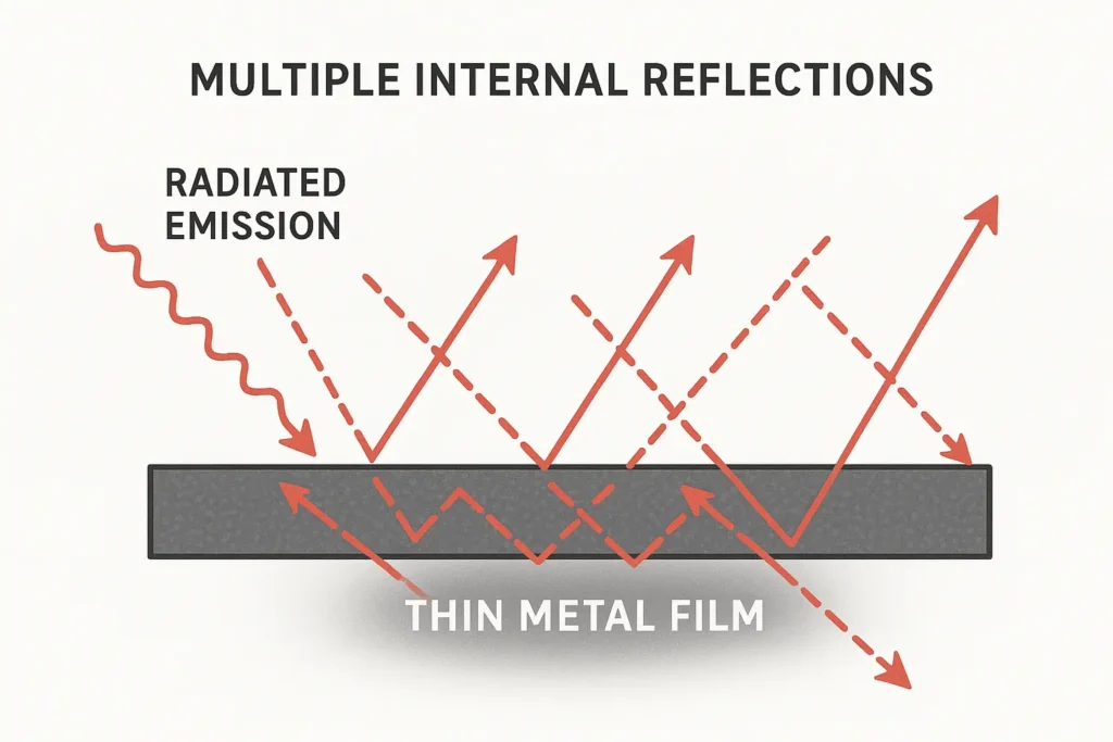
- Enhanced absorption through defect engineering: Thermal evaporation, especially when parameters are not optimized for dense films, can result in a higher density of defects, such as grain boundaries, crystal imperfections, and localized voids. These defects, while detrimental to bulk conductivity, can significantly increase the conversion of electromagnetic energy into thermal energy, a process known as dielectric loss. The trapping and scattering of waves within this disordered structure amplify this absorption effect.
- Reduced reflection: The increased absorption within the film can lead to a desirable reduction in reflection (SER) compared to perfect metal sheets, which can cause secondary EMI pollution. By trapping and neutralizing the radiation, the film minimizes the re-emission of waves that could interfere with nearby devices.
- Optimized conductivity: A metal’s conductivity is typically reduced as the film thickness drops below 100 nanometers. In thermally evaporated films, this reduced conductivity shifts the balance of shielding from pure reflection towards absorption. This allows even very thin films, such as a 6.5 nm gold film, to achieve significant absorption by reducing the electrical impedance mismatch that causes high reflection in thicker, more conductive films.
Factors influencing radiation trapping
The degree of innate radiation trapping can be tuned by controlling the thermal evaporation process and subsequent material properties:
- Film morphology and porosity: The inherent structure of the deposited film is crucial. By adjusting deposition parameters like substrate temperature and vacuum pressure, one can control the film’s porosity and nanostructure, directly impacting the degree of multiple scattering and absorption.

Thermal Evaporated NiCr over Cu illustration of nanostructured film.
- Film thickness: As demonstrated by thin-film research, decreasing the film thickness can reduce conductivity and promote absorption over reflection, as long as a sufficiently continuous, though nanostructured, film is maintained.
- Metal selection: The choice of metal influences conductivity and magnetic permeability, which are key factors in both reflection and absorption-based shielding. For example, combining a high-conductivity metal like copper with a magnetic material can create synergistic effects that enhance absorption.
This innate radiation trapping mechanism explains how thermally evaporated thin films can achieve substantial EMI shielding despite not being perfectly dense or having high bulk conductivity. By embracing the intrinsic defects and morphology of the thermal evaporation process, engineers can design lightweight, ultra-thin, and flexible shielding materials with absorption-dominant properties for next-generation electronics. This is particularly useful for applications requiring minimal size and weight (eg medical and aerospace/defense applications).